Tech Insight: Chiplet Architecture & The Future of Semiconductor Manufacturing in 2026
The semiconductor landscape is undergoing its most significant shift in a decade. As we close out 2025, the industry buzz isn't just about smaller nanometers anymore, it is about Chiplet Architecture.
For years, "Monolithic" design (one single, massive silicon die) was the standard. But as we look toward the 2026 hardware roadmap, the limitations of physics and cost are pushing manufacturers toward a modular future.
Here is why Chiplet Architecture is set to dominate 2026 and why this architecture is the game-changer for AI, High-Performance Computing (HPC), and Consumer Electronics.
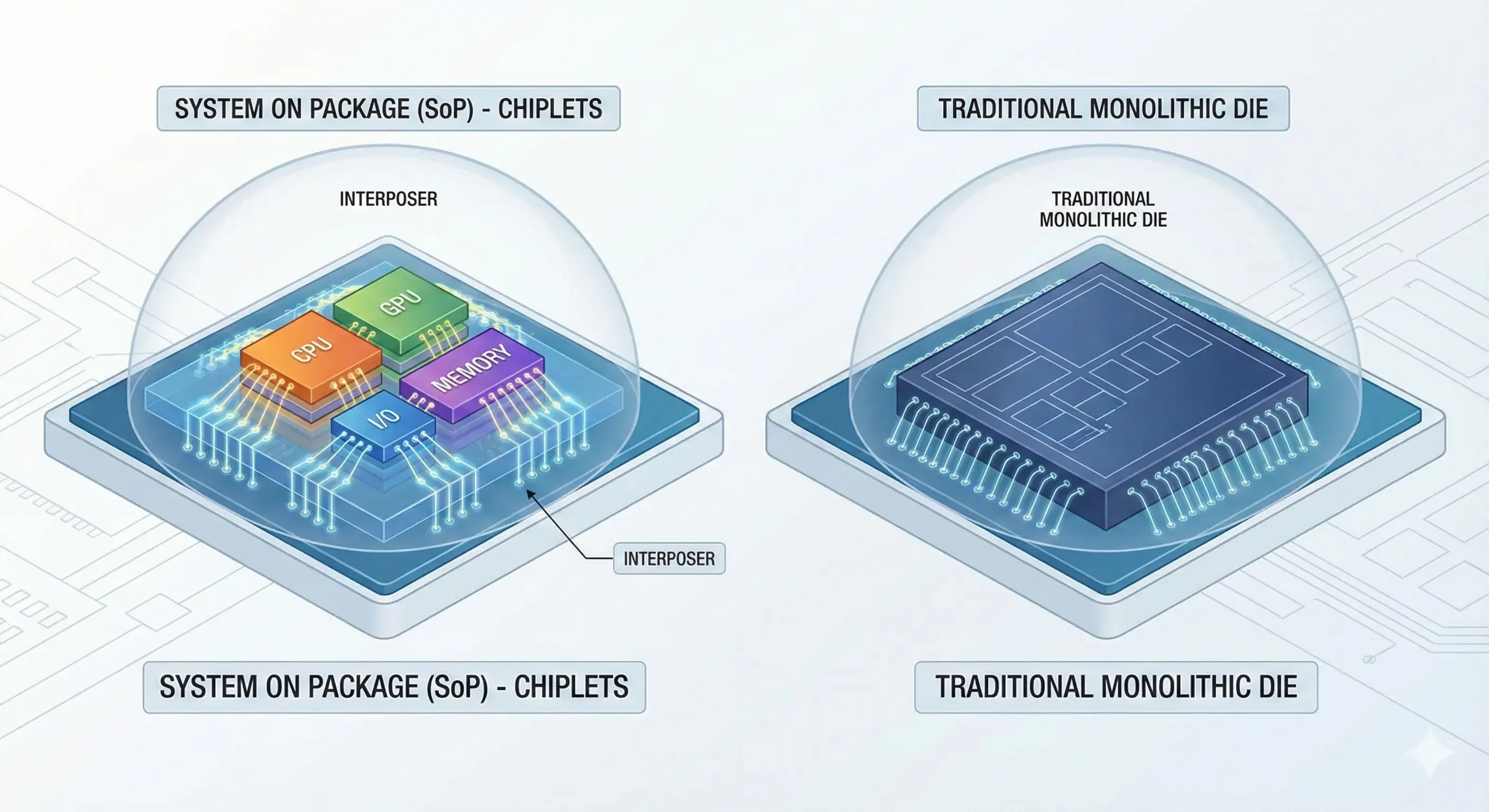
The End of "One Big Chip": Monolithic vs. Chiplet
As highlighted in our previous Tech Insights, the traditional approach of cramming billions of transistors onto a single large die is hitting a wall. The problem? Yield and Cost.
When you manufacture a massive monolithic chip, a single microscopic defect can render the entire processor useless. This waste is incredibly expensive at advanced nodes (like 2nm or 1.8nm).
To understand the shift, let's compare the two approaches:
| Feature | Monolithic Design (Traditional) | Chiplet Architecture (Future Standard) |
|---|---|---|
| Design Structure | Single, large silicon die | Multiple smaller dies (Chiplets) connected |
| Manufacturing Cost | High (Exponentially higher at <3nm) | Lower (Optimized silicon utilization) |
| Yield Rate | Low (One defect kills the whole chip) | High (Defective chiplets are discarded individually) |
| Flexibility | Fixed process node for all components | Heterogeneous Integration (Mix & match nodes) |
| Time-to-Market | Slow (Full redesign required) | Fast (Modular upgrades) |
The Modular Solution: Yield and Cost Efficiency
Chiplet Architecture solves the monolithic yield problem by going modular. Instead of one giant chip, engineers break the design into smaller, distinct functional blocks.
- Deconstruction: The design is split into CPU, GPU, I/O, and Cache modules.
- Yield Improvement: Smaller dies are statistically easier to manufacture without defects. If one small chiplet is bad, you discard only that piece—not the whole package.
- Cost Efficiency: This modularity significantly lowers production costs while maximizing silicon utilization, a key factor in Semiconductor Manufacturing profitability.
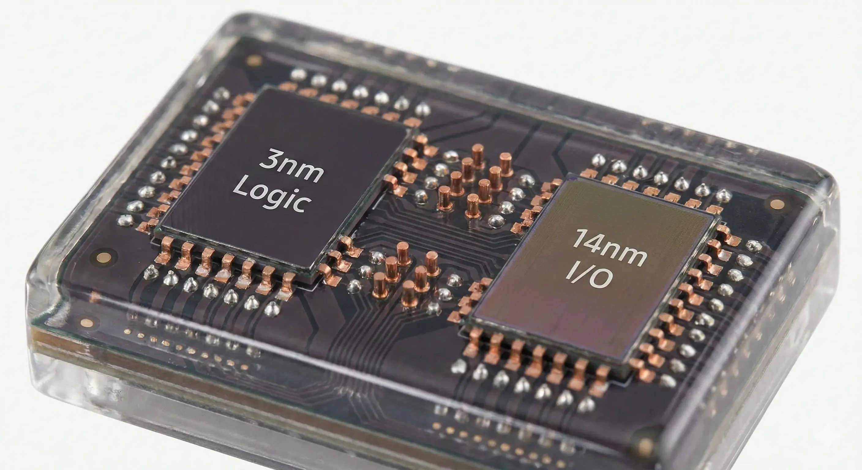
Customization: The "Lego" Approach to Heterogeneous Integration
One of the key drivers for 2026 is Heterogeneous Integration. In a monolithic design, every part of the chip must be built using the same manufacturing process. This is inefficient.
With chiplets, manufacturers can mix and match process nodes to optimize performance and cost:
- Logic Core (CPU/GPU): Built on cutting-edge 3nm or 2nm nodes for maximum speed.
- I/O & Analog: Built on mature, cost-effective 14nm or 28nm nodes.
This flexibility allows for hyper-specialized chips tailored for specific industries, from AI accelerators to Electric Vehicle (EV) systems, without the massive price tag of a fully advanced monolithic die.
The Interconnect Wars: UCIe and Standards
A chiplet system is only as fast as the connection between its parts. If data cannot move between chiplets instantly, performance stalls. This is where Interconnect Technology becomes critical.
In 2026, we are seeing the rise of open standards endorsed by bodies like JEDEC and the UCIe Consortium:
- UCIe (Universal Chiplet Interconnect Express): Rapidly becoming the industry standard (the "USB of chiplets"). It offers high bandwidth and low latency, enabling an open ecosystem where chiplets from different vendors can work together seamlessly.
- Advanced Packaging (2.5D & 3D): Technologies like CoWoS (Chip-on-Wafer-on-Substrate) and Hybrid Bonding are reducing the physical distance signals must travel. As noted in our recent breakdown: "Shorter distance = Faster signals + Lower power."
Why This Matters for 2026 Devices
What does this mean for the end-user and the market in 2026?
- AI Everywhere: Chiplets allow for massive memory bandwidth (essential for LLMs) by stacking memory directly on top of compute units using 3D IC Integration.
- Thermal Management: Breaking up a hot monolithic chip into spread-out chiplets helps dissipate heat more effectively, reducing thermal throttling in high-performance devices.
- Faster Time-to-Market: Companies can upgrade specific modules (like the NPU for AI) while keeping the rest of the chip design the same, speeding up release cycles.
Conclusion: The Future is Modular
The shift to Chiplet Architecture is not just a trend; it is the foundation of the 2026 semiconductor standard. By moving from monolithic to modular, the industry is achieving better yields, lower costs, and higher customization.
For manufacturers and engineers, the focus must now shift to Advanced Packaging and Interconnect efficiency. The era of the single giant chip is fading. The era of the high-performance team of chiplets has arrived.
Interested in deep-diving into semiconductor manufacturing trends? Contact our Engineering Team to discuss how these shifts impact your hardware roadmap.